Call +1(917) 993 7467 or connect with one of our experts to get full access to the most comprehensive and verified construction projects happening in your area. 

Last Updated on 22nd August 2024
Taiwan Semiconductor Manufacturing Company (TSMC), one of the largest semiconductor manufacturing companies in the world, breaks ground on a USD 11 billion semiconductor fabrication plant in Dresden, Germany. A joint venture between TSMC, Robert Bosch GmbH, Infineon Technologies AG, and NXP Semiconductors developed the semiconductor fabrication plant in Germany.
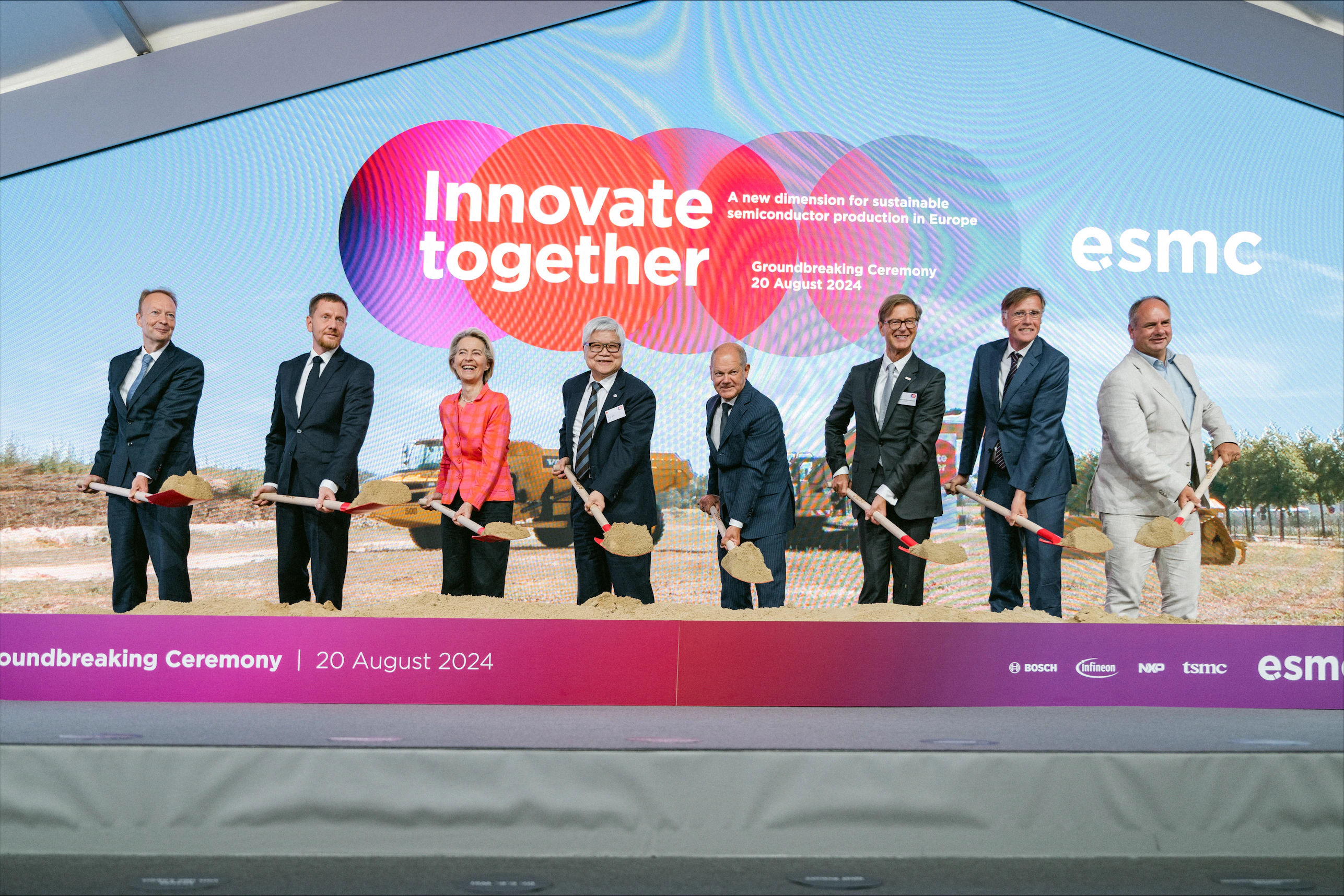
Dresden Fab Groundbreaking Ceremony
When fully operational, the fabrication plant is expected to have a monthly production capacity of 40,000 300-mm (12-inch) wafers on TSMC’s 28/22 nanometer planar CMOS and 16/12 nanometer FinFET process technology. This will further strengthen Europe’s semiconductor manufacturing ecosystem with advanced FinFET transistor technology. The plant will manufacture microcontroller units used in cars, such as windows, brakes, and sensors.
The Dresden fab is TSMC’s first fab in Germany. The groundbreaking ceremony will officially mark the initial land preparation phase for the new facility, which is expected to generate around 2,000 direct high-tech professional jobs. Additionally, each direct job created by the project is expected to stimulate the creation of numerous indirect jobs throughout the EU supply chain, bolstering the region’s economy.
Total investments are expected to exceed USD 11 billion. These investments include equity injections, debt borrowing, and strong support from the European and German governments. The EU Commission has approved USD 5 billion for the semiconductor fabrication project.
The FinFET (Fin Field Effect Transistor) process is a 3D process adopted to overcome the limitations of conventional planar (2D) structures. The structure looks like a fish’s fin, hence ‘Fin’FET.
FinFETs are primarily used in home computers, laptops, tablets, smartphones, wearables, and high-end networks. They are also used in microchips and are the dominant gate design for 7 nm, 10 nm, and 14 nm process nodes.
Read: TSMC to Invest $65 Billion for the Development of Semiconductor Factories in Arizona, USA
Subscribe to the upcoming and ongoing Semiconductor Fabrication projects and tenders database in Germany to access reliable and high-quality insights on forthcoming, in-progress, and completed Semiconductor Fabrication plant projects across Germany.
Our user-friendly platform provides essential details, timely updates, key stakeholder contact information, and business opportunities tailored for engineering companies, industry professionals, investors, and government agencies.
Start a free demo to learn about the latest Semiconductor fabrication projects in Europe and take your business to the next level!

News_Release 10th Nov 2023

News_Release 20th Nov 2023

News_Release 21st Nov 2023

News_Release 23rd Nov 2023

News_Release 23rd Nov 2023

News_Release 28th Nov 2023
