Call +1(917) 993 7467 or connect with one of our experts to get full access to the most comprehensive and verified construction projects happening in your area. 

Last Updated on 25th June 2024
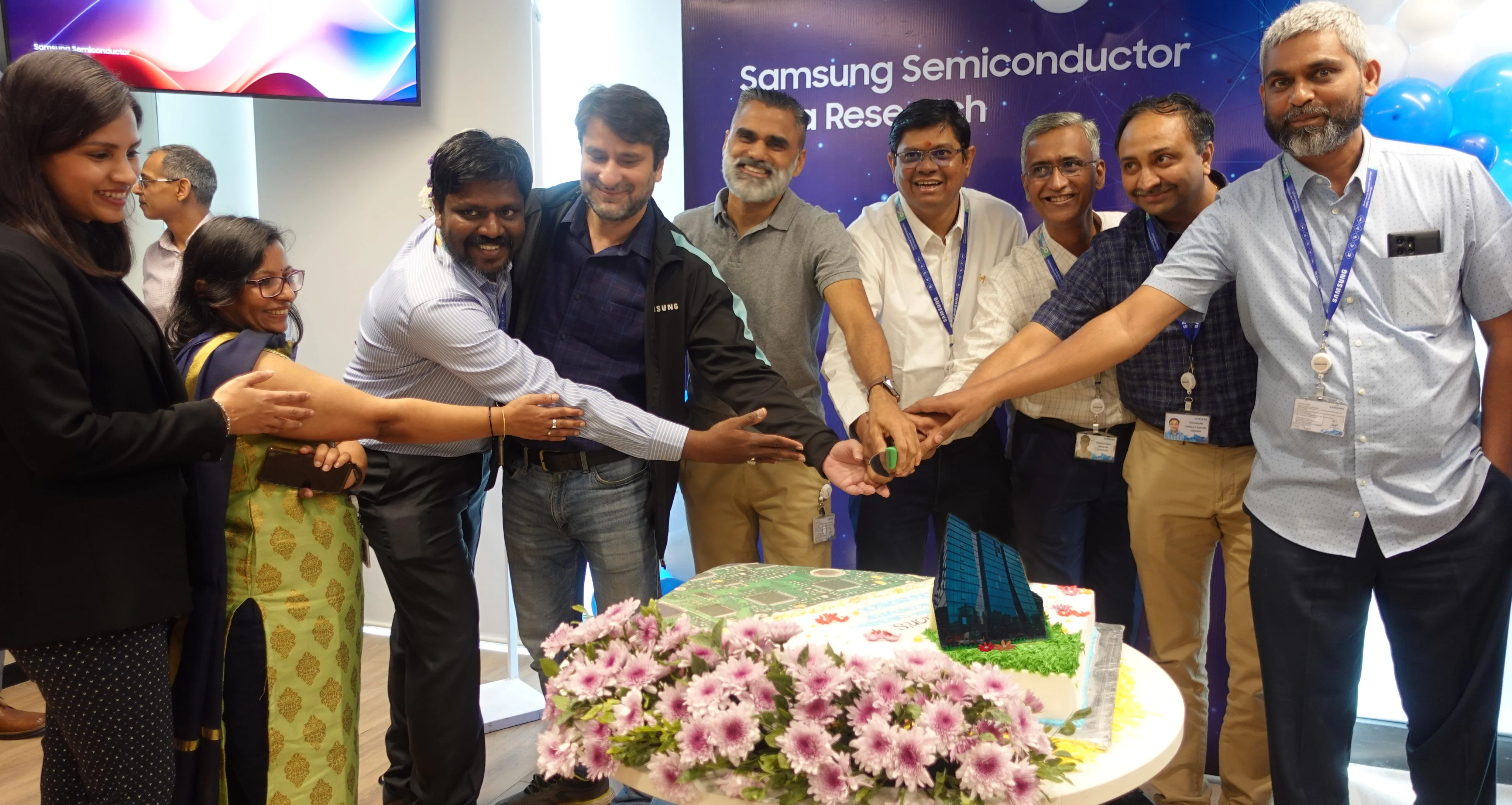
Samsung Semiconductor India Research (SSIR) has inaugurated a new research and development (R&D) facility in Bengaluru, marking a significant milestone in the company's commitment to advancing semiconductor research in India. This new facility, SSIR's second office in Bengaluru, is designed to accommodate about 1,600 professionals.
The new R&D center is located at Bagmane Capital Tech Park in Angkor-West and spans 1.6 lakh square feet across four floors. The facility features an open-plan layout, encouraging collaboration and agility. It includes designated hot-desking areas for workforce flexibility and over 60 state-of-the-art meeting rooms for seamless communication.
Balajee Sowrirajan, EVP & MD at Samsung Semiconductor India Research, expressed his excitement about the new facility. He stated that the new hub embodies Samsung's commitment to expanding its footprint in India and enabling a vibrant environment for its exceptional team members. This new hub reinforces SSIR's standing as a crucial player in Samsung Semiconductor’s global innovation ecosystem.
SSIR currently has over 4,500 employees and plans to add over 700 people, including fresh graduates and lateral hires across teams in India. This expansion is a testament to Samsung's commitment to driving cutting-edge semiconductor research and development in India while addressing the company's growing need for advanced infrastructure.
Driving Semiconductor R&D in India: The primary objective of this new facility is to drive cutting-edge semiconductor research and development in India. Semiconductors are the backbone of modern electronics, including computers, smartphones, and other digital devices. By focusing on semiconductor R&D, Samsung aims to stay at the forefront of technological innovation.
Addressing Infrastructure Needs: The new R&D center is designed to address the company's growing needs for advanced infrastructure. With modern and open-plan layouts across four floors, the facility encourages enhanced collaboration and flexibility for its employees.
Enhancing the Global Innovation Ecosystem: The new hub reinforces SSIR's standing as a crucial player in Samsung Semiconductor’s global innovation ecosystem. By establishing this new facility, Samsung aims to open doors to new opportunities and foster innovation.
In conclusion, the establishment of the new R&D facility in Bengaluru is a strategic move by Samsung to drive semiconductor research in India, expand its workforce, enhance its infrastructure, and foster a vibrant work environment. This step not only reinforces SSIR's crucial role in Samsung Semiconductor’s global innovation ecosystem but also underscores Samsung's commitment to expanding its footprint in India.
Samsung Semiconductor India Research (SSIR) is a part of the global network of Samsung Electronics Co., Ltd. It provides component solutions, featuring industry-leading technologies in the areas of system LSI, memory, and foundry in the Asia Pacific region. SSIR has a state-of-the-art research and development (R&D) center in Bengaluru, India. This facility is aimed at driving cutting-edge semiconductor research and development in India, addressing the company's growing need for advanced infrastructure.
Are you looking for a platform that gives you reliable, high-quality, and timely project insights for semiconductor manufacturing projects across India?
Discover the Global Project Tracking (GPT) platform by Blackridge Research, designed to provide you with the most recent Indian Semiconductor Fabrication Plant Projects and Tenders better and faster across various stages of development:
The user-friendly interface helps you obtain early-stage awareness of projects and find the right business opportunity quickly.
Each project will have all the essential details, such as scope, capacity, CapEx, status, project description, companies involved, funding information, location, periodic updates, important event dates like construction start date, commissioning dates, and key contact information of project owners and stakeholders.
The database is a vital resource for a wide range of entities, including semiconductor manufacturers, EPC Companies, silicon material suppliers, data analytics and software providers, consulting and advisory firms, investors, multilateral banks and financial institutions, and law firms

News_Release 10th Nov 2023

News_Release 20th Nov 2023

News_Release 21st Nov 2023

News_Release 23rd Nov 2023

News_Release 23rd Nov 2023

News_Release 28th Nov 2023
