Call +1(917) 993 7467 or connect with one of our experts to get full access to the most comprehensive and verified construction projects happening in your area. 

Last Updated on 25th June 2024
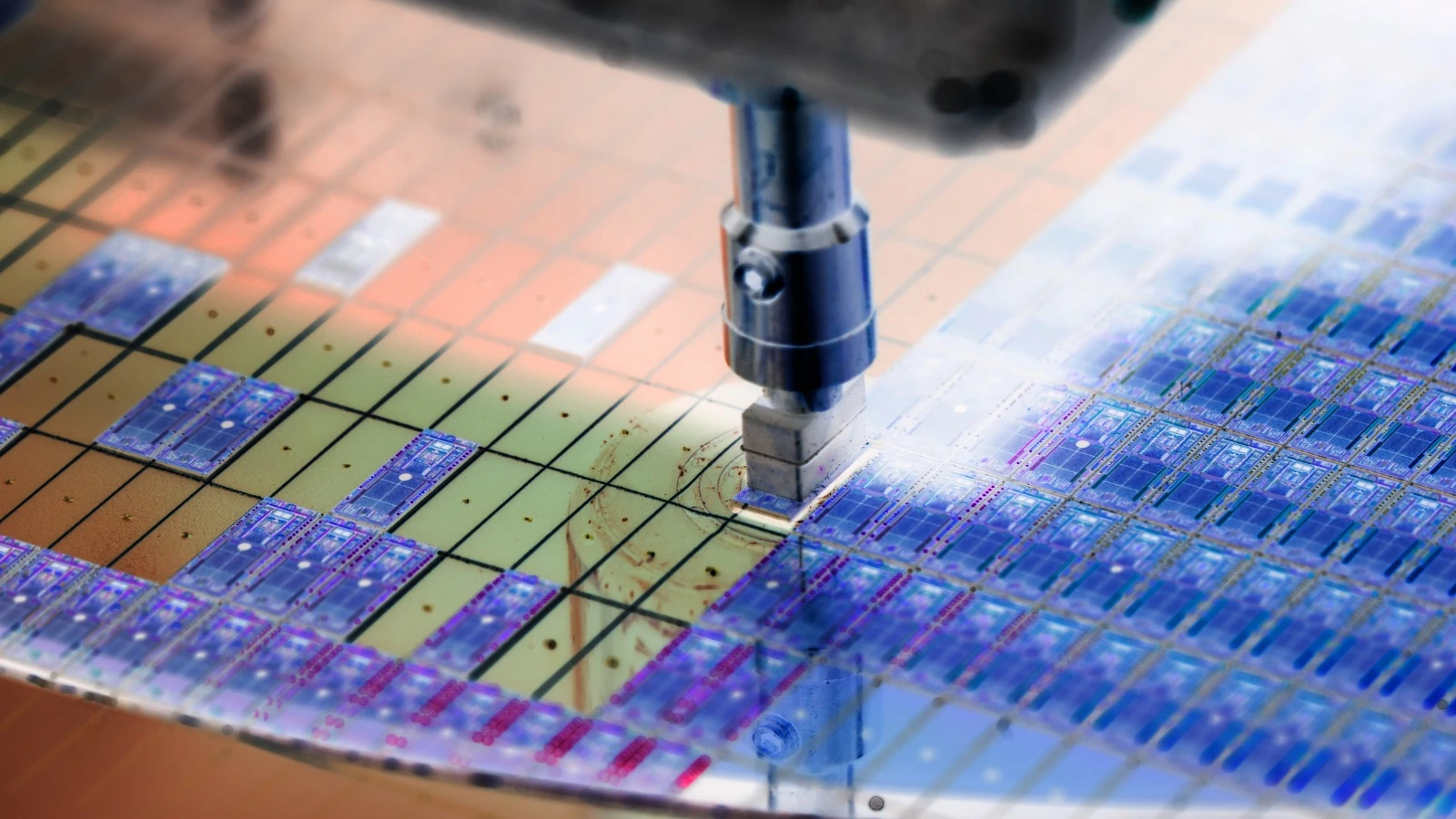
New York State will establish a USD 10 billion next-generation semiconductor research and development center at the NY CREATES (the New York Centre for Research, Economic Advancement, Technology, Engineering, and Science) Albany NanoTech Complex. The partnership includes major players in the semiconductor industry, such as IBM, Micron, Applied Materials, and Tokyo Electron.
These entities intend to break new ground in semiconductor manufacturing technologies, adhering to new market trends. New York State Governor Kathy Hochul stated that the USD 10 billion partnership will bring innovative chip research and development to the entire industry.
This collaboration will support the long-term expansion of New York's technology economy, generate and retain thousands of direct, indirect, and union construction jobs, and establish the most advanced, publicly owned semiconductor R&D infrastructure in the nation within New York State.
Additionally, the partnership will fund the development of a cutting-edge High NA Extreme Ultraviolet Lithography Center, which will support the research and development of the world’s most complex and powerful semiconductors.
To support this project, New York State will fund USD 1 billion to expand the Albany NanoTech Complex. The state will construct a NanoFab Reflection that covers 50,000 square feet of clean room space. Furthermore, NYCREATES will acquire a high-NA EUV lithography tool from ASML. Once operational, New York’s High NA EUV Center will be a destination for research and development of innovative chip technology.
Earlier in October 2022, the Governor unveiled a landmark USD 100 billion investment from Micron, following the ratification of New York's pioneering Green CHIPS legislation aimed at fostering a sustainable and prosperous chip industry. Micron's investment will construct a cutting-edge, state-of-the-art memory manufacturing campus in Central New York, eventually generating 50,000 employment opportunities.
| What is a high-NA EUV lithography tool? |
| A high-NA EUV lithography tool is a cutting-edge piece of equipment used to create the incredibly tiny circuits found in modern computer chips. It stands for High-Numerical-Aperture Extreme Ultraviolet Lithography, and it represents a significant leap forward in chip manufacturing technology. |
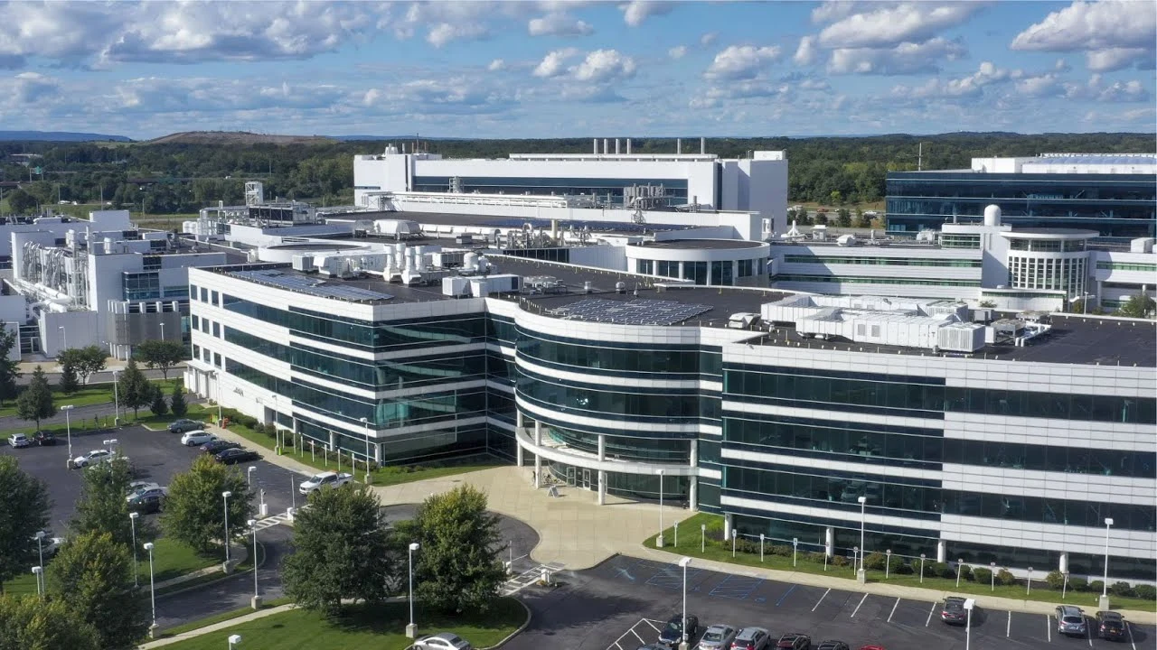
NY CREATES stands for the New York Center for Research, Economic Advancement, Technology, Engineering, and Science. It's a world-leading R&D, innovation hub, and commercialization facilitator focused on advanced digital, analog, and power technologies.
With over two decades of experience in semiconductor innovation, NY CREATES is the most sophisticated publicly owned 300 mm semiconductor R&D facility in North America. The facility houses current-generation EUV lithography equipment. IBM utilized this equipment to fabricate the world's first two-nanometer chip technology. The new High NA EUV Center will solidify New York's position as the epicenter of cutting-edge semiconductor research and development.
| What is the Green CHIPS legislation? |
| The Green CHIPS legislation, formally known as the Green Chips Manufacturing Tax Credit Program Act, is a groundbreaking initiative by the state of New York to attract and incentivize semiconductor manufacturing within its borders. Signed into law by Governor Kathy Hochul in August 2022. |
Are you looking for a platform that gives you reliable, high-quality, and timely project insights for Semiconductor Manufacturing Projects in US?
Discover the Global Project Tracking (GPT) platform by Blackridge Research, designed to provide you with the most recent US Semiconductor Fabrication Plant Projects and Tenders better and faster across various stages of development:
The user-friendly interface helps you obtain early-stage awareness of projects and find the right business opportunity quickly.
Each project will have all the essential details, such as scope, capacity, CapEx, status, project description, companies involved, funding information, location, periodic updates, important event dates like construction start date, commissioning dates, and key contact information of project owners and stakeholders.
The database is a vital resource for a wide range of entities, including semiconductor manufacturers, EPC Companies, silicon material suppliers, data analytics and software providers, consulting and advisory firms, investors, multilateral banks and financial institutions, and law firms.
Book a Free demo to learn more about the US Semiconductor Fab Projects and Tenders database and how we can help you achieve your goals.

News_Release 10th Nov 2023

News_Release 20th Nov 2023

News_Release 21st Nov 2023

News_Release 23rd Nov 2023

News_Release 23rd Nov 2023

News_Release 28th Nov 2023
