Call +1(917) 993 7467 or connect with one of our experts to get full access to the most comprehensive and verified construction projects happening in your area. 

Last Updated on 25th June 2024
Amkor Technology has declared its plan to construct a state-of-the-art packaging and testing facility in Peoria, Arizona. In a press release, Amkor stated that the company plans to invest USD 2 billion to complete the project. The new facility will provide direct employment opportunities for 2,000 people.
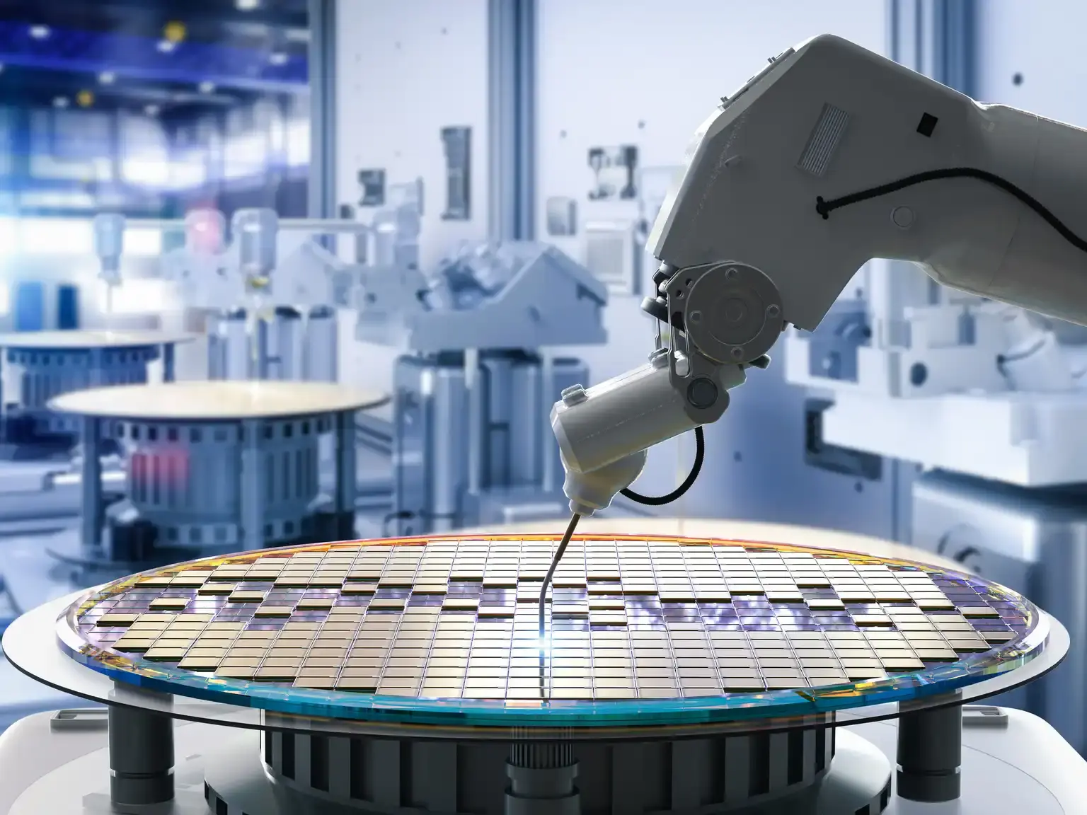
The company has acquired an estimated 55 acres of land to construct the new cutting-edge manufacturing campus, which will feature over 500,000 square feet of clean room space. Amkor is the only US-headquartered OSAT (outsourced semiconductor assembly and testing) service provider with advanced packaging technology. This new facility will be the largest outsourced advanced packaging facility in the US.
Amkor will package and test chips manufactured for Apple at the adjacent TSMC fab. Once the new facility is operational, Apple will be Amkor’s first and largest customer. Amkor has applied for CHIPS funding in order to guarantee the success of a venture of this scale in the United States. Earlier this month, the Commerce Department unveiled its plans to spend USD 3 billion on advanced packaging and manufacturing.
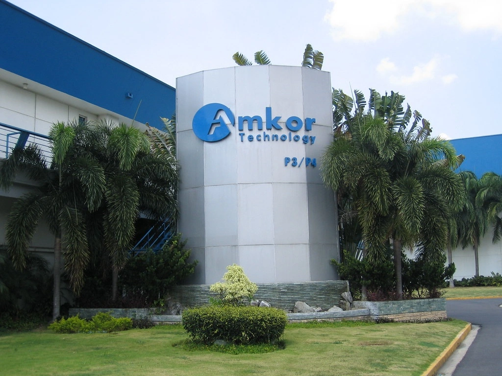
Amkor Technology, Inc. is a global leader in the semiconductor packaging and test services industry. The company was founded in 1968 and is headquartered in Tempe, Arizona, USA. Amkor has over 20,000 employees worldwide and operates semiconductor production facilities in Asia, EMEA, and the USA.
Amkor's customers include some of the world's largest semiconductor companies, such as Intel, Samsung, and Qualcomm. The company is also a supplier to a wide range of other industries, including consumer electronics, automotive, and industrial.
Here are some notable semiconductor projects undertaken by Amkor Technology:
The CHIPS and Science Act of 2022 is a United States federal law that provides $52.7 billion in funding for semiconductor manufacturing, research and development, and workforce training in the United States. On August 9, 2022, President Joe Biden signed the Act into law. The Act's main goals are to:
The Act includes several key provisions, including:
Are you looking for a platform that gives you reliable, high-quality, and timely project insights for Semiconductor Manufacturing Projects in India?
Discover the Global Project Tracking (GPT) platform by Blackridge Research, designed to provide you with the most recent US Semiconductor Fabrication Plant Projects and Tenders better and faster across various stages of development:
The user-friendly interface helps you obtain early-stage awareness of projects and find the right business opportunity quickly.
Each project will have all the essential details, such as scope, capacity, CapEx, status, project description, companies involved, funding information, location, periodic updates, important event dates like construction start date, commissioning dates, and key contact information of project owners and stakeholders.
The database is a vital resource for a wide range of entities, including semiconductor manufacturers, EPC Companies, silicon material suppliers, data analytics and software providers, consulting and advisory firms, investors, multilateral banks and financial institutions, and law firms.
Book a Free demo to learn more about the US Semiconductor Fab Projects and Tenders database and how we can help you achieve your goals.

News_Release 10th Nov 2023

News_Release 20th Nov 2023

News_Release 21st Nov 2023

News_Release 23rd Nov 2023

News_Release 23rd Nov 2023

News_Release 28th Nov 2023
