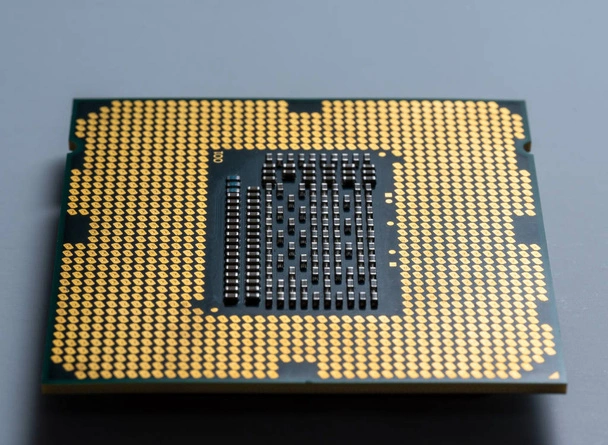
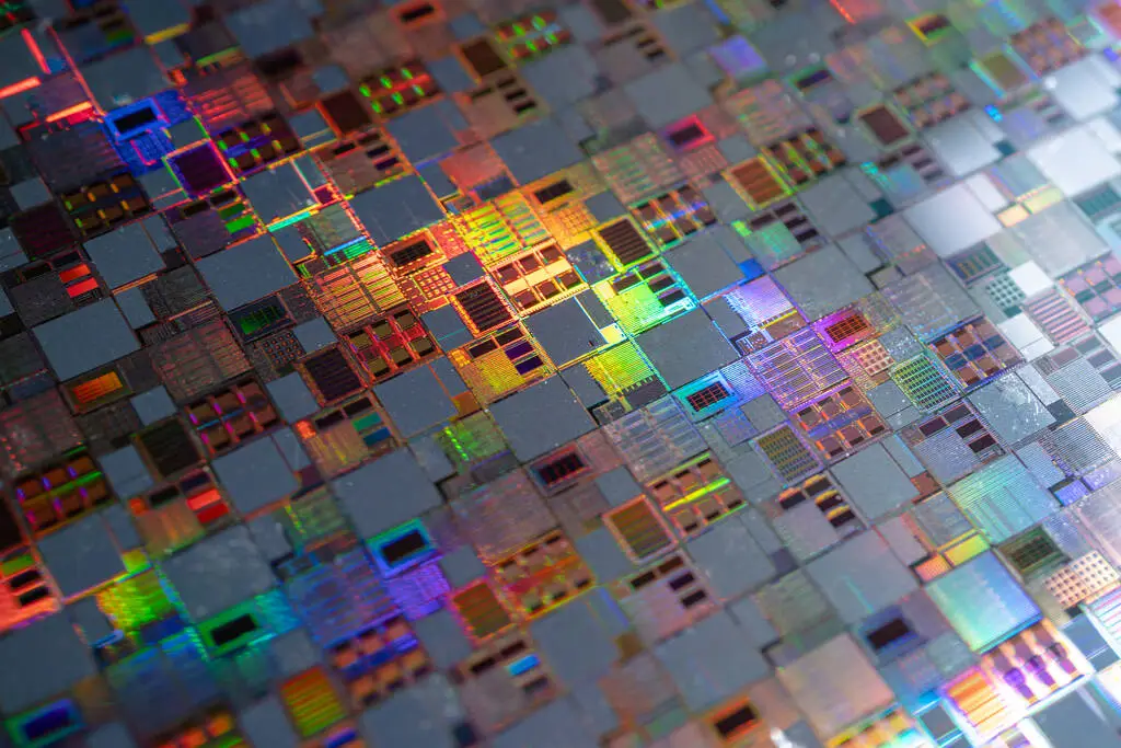
The semiconductor wafer fabrication process converts raw materials like silicone, germanium, and gallium arsenide into small chips. The process of wafer fabrication inlcudes steps like wafer preparation, pattern transfer, doping, deposition, etching, and packaging. It is the first step in manufacting semiconductors.

Before exploring the first step in the semiconductor manufacturing process, it is important to know what a semiconductor is?
What is a Semiconductor?
A substance with certain electrical properties that make it appropriate for use as the foundation for computers and other electronic devices is a semiconductor or an integrated circuit (IC). It can be a solid chemical element or compound that, under specific conditions, transmits electricity into the surrounding environment.
Read: A Comprehensive Guide to the Fabless Semiconductor Industry
What is a Wafer?
A semiconductor wafer is a thin piece of semiconductor material, such as crystalline silicon, utilized in semiconductor manufacturing. Wafers are circular, and their diameter can vary from a few millimeters to many inches. They are carefully polished to achieve a surface as reflective as a mirror and completely free of impurities.

Find Semiconductor Fab plant Projects & Tenders across the WorldClaim your free leads!
Wafer Fabrication Process
Semiconductor wafers serve as the fundamental basis for integrated circuits and semiconductor devices. They are manufactured through a complex multi-step procedure. Now let us go through the essential stages of converting an unprocessed semiconductor material into a refined wafer prepared for electronic device manufacturing.
Ingot Growth
The process starts with the development of a crystal silicon ingot. A little silicon seed crystal is inserted into a quartz crucible filled with liquefied polysilicon. The crucible is gradually removed from the liquid silicon during the extraction process. The seed crystal serves as a model for the molten polysilicon to solidify around, forming a single crystal ingot that can reach up to 2 meters. The process needs meticulous control over temperature gradients and extraction rates, to grow flawless crystalline formations.
Slicing
The grown cylindrical ingot is divided into thin discs by using a specialized saw equipped with a cutting blade infused with diamonds. A single ingot can yield hundreds of round wafers. During the process of sawing, the thickness of the wafer is carefully regulated to ensure consistency and facilitate subsequent stages of processing. At this point, the thickness of the wafers usually ranges from 500 to 900 microns.
Edge Grinding
Due to the formation of minor cracks and imperfections during the cutting process, it is necessary to smooth out the periphery of the wafer. During the edge grinding process, wheels are used to eliminate a thin strip of material from the edge. It is done until a pristine, unblemished "new" edge surface is achieved along the whole circumference of the wafer.
Read: Photolithography: The Art of Pattern Transfer in Semiconductor Fabrication Process
Lapping
Next, the wafer surface undergoes a global planarization procedure known as lapping. The wafers gradually rotate between two revolving cast iron plates coated with an abrasive slurry. The plates remove material from the front and back wafer surfaces until they achieve a flat and parallel configuration. Lapping is a process that eliminates saw marks from wafer slicing. It also brings the wafer thickness very close to the desired thickness for device fabrication.
Etching
Following the lapping procedure, the wafers still have surface degradation and impurities accumulated from prior procedures. Etching is conducted by using aqueous solutions containing a combination of hydrofluoric, nitric, and acetic acids. These chemicals selectively and uniformly eliminate a small number of microns off the surface of a silicon wafer. It simultaneously eliminates any imperfections, resulting in a flawless surface layer.
Polishing
At this point, the wafers undergo a mechanical-chemical polishing process where a silica-based slurry is used. This slurry oxidizes the silicon surface while abrasive particles and a soft pad physically remove it. Integrating chemical and mechanical polishing techniques results in highly polished wafer surfaces that resemble mirrors, free from any damage. These smooth surfaces are crucial for photolithography and subsequent procedures.
Cleaning
After polishing, wafers are subjected to extensive cleaning in wet chemical baths. This is done to eliminate particles, organic pollutants, and metal impurities from the surfaces of the wafers. It is done to ensure that all the cleanliness standards are upheld. Diverse analytical techniques are employed to examine, monitor, and assess the wafers before they are sent to the facilities for device production.
Read: A Comprehensive Guide to Deposition Techniques in Semiconductor Fabrication
Types of semiconductor wafers
Wafers used in semiconductor manufacturing are available in various types, each with its own characteristics and applications. Silicon, germanium, and gallium arsenide are the three varieties that are present most frequently.
Silicon wafers
Silicon wafers are widely used to fabricate semiconductors, electronic components, microchips, and solar cells. Additionally, they are utilized in fabricating micro-electromechanical systems (MEMS), found in electronic devices and sensors.
Germanium wafers
Germanium wafers are utilized to produce high-frequency transistors and other electronic components. They may be used in infrared detectors and other optical devices.
Gallium arsenide wafers
Gallium arsenide wafers are widely used to fabricate high-speed transistors and various other electronic components. Additionally, they are used to produce solar cells and other electronic equipment that necessitate optimal efficiency.
Find Semiconductor Fab Plant
Projects & Tenders across the World Claim your free leads!
Challenges in Wafer Fabrication
The semiconductor industry faces several challenges, including:
- Miniaturization: It is becoming increasingly challenging to maintain precision in patterning and etching as the size of the devices continues to decrease.
- Yield Optimization: To achieve cost efficiency, maximizing the number of functional chips produced from a single wafer is essential. This necessitates constantly improving the process control.
- Material Innovation: Ongoing research is being conducted to develop new materials capable of satisfying the requirements of modern semiconductor devices.
Innovations and Future Directions
The semiconductor industry continuously evolves, driven by the need for more powerful and efficient devices. Innovations include:
- Extreme Ultraviolet (EUV) Lithography: EUV lithography makes it possible to use smaller feature sizes and manufacture advanced nodes that are larger than 7 nanometers.
- 3D Integration: There is a substantial potential for performance and density enhancement through the stacking of many layers of semiconductors.
- Quantum Computing: Techniques for fabricating semiconductors are being modified to produce qubits for quantum computers, which has the potential to revolutionize computing power.
Read: Semiconductor Market Trends: What to Expect in the Coming Years
How to choose the right semiconductor wafer?
Choosing a suitable semiconductor wafer for a particular application can be challenging. The process involves recognizing the properties of different semiconductor materials and the manufacturing techniques employed to produce them. Furthermore, it involves understanding the application's needs and choosing the semiconductor wafer most effectively meets those criteria.
When considering this selection, it is important to consider many elements such as the material, dopant concentration, thickness, and quality of the wafer. Additionally, it is important to evaluate the expense of the wafer and the accessibility of the material.
Read: What is A Cleanroom and Why is It Important in Semiconductor Production?
Conclusion
The semiconductor wafer fabrication process is intricate and includes various additional steps, such as ingot growth, slicing, edge grinding, lapping and other specialized processes. These processes vary based on the specific requirements of the integrated circuits being produced. The procedure is carried out in specialized facilities called semiconductor fabs or foundries, which demand precisely controlled surroundings and sophisticated machinery.
Thus, wafer fabrication is an essential component of the semiconductor manufacturing process. It establishes the foundation for the production of electronic devices of superior quality. Producers can guarantee that their wafers satisfy the rigorous criteria essential for fabricating dependable and high-performance semiconductor devices through meticulous regulation of the crystal growth, wafer slicing, polishing, and cleansing procedures.
Frequently Asked Questions
Here are some frequently asked questions about the topic,
Why are silicon wafers used in semiconductor fabrication?
Silicon wafers are frequently used as substrate materials in the fabrication of semiconductors owing to their cost-effectiveness, abundant availability, and exceptional electrical conductivity. Furthermore, silicon exhibits exceptional compatibility with a wide range of fabrication processes and can be readily doped with impurities in order to alter its electrical properties.
How is quality control maintained in the semiconductor fabrication process?
Inspection, measurement, and evaluation methods are utilized to maintain quality control, including wafer inspection, electrical testing, and reliability assessment. These techniques facilitate the detection and rectification of flaws, enhance process regulation, and uphold superior manufacturing outputs to guarantee that the ultimate semiconductor devices fulfill their performance and reliability criteria.
How many chips can be created per wafer?
Approximately 300-400 chips can be produced from a 300mm wafer with a diameter of 12 inches, with the precise quantity dependent upon the dimensions of the die and the inter-chip spacing. Producing high-quality semiconductors requires meticulous attention to detail and a highly complex procedure.
What is the difference between a chip and a wafer?
The correlation between wafers and chips constitutes the difference between the two. Although the wafer functions as a foundation for the chip, the chip itself is inserted into the wafer. Collectively, they constitute an essential component that is frequently used in the field of electronics.
Connect with Decision-makers of the Latest Semiconductor Fabrication Plant Projects Around the World with Ease.
Subscribe to our database for latest Semiconductor plants and tenders around the world to get access to reliable and high-quality insights on upcoming, in-progress, and completed semiconductor projects across the world or in your desired geographical location.
Our user-friendly platform provides essential details, timely updates, key stakeholder contact information, and business opportunities tailored for engineering companies, industry professionals, investors, and government agencies.
Start a free demo to take your business to the next level!


Leave a Comment
We love hearing from our readers and value your feedback. If you have any questions or comments about our content, feel free to leave a comment below.
We read every comment and do our best to respond to them all.